hello दोस्तों आज हम इस पोस्ट में Block diagram & architecture of 8085 Microprocessor in hindi (8085 माइक्रोप्रोसेसर के ब्लॉक डायग्राम और आर्किटेक्चर) को विस्तारपूर्वक पढेंगे तो चलिए शुरू करते है:-
टॉपिक
Block diagram of 8085 Microprocessor in hindi –architecture
8085 microprocessor एक 8 bit माइक्रोप्रोसेसर है जिसको NMOS तकनीक का प्रयोग करके 1977 में intel ने विकसित किया था. यह कंप्यूटर का CPU (central processing unit) होता है.
इसके पास निम्नलिखित configuration होते है:-
- इसमें 8 bit data bus होती है.
- 16 bit address bus होती है जो कि 64 kb से ज्यादा को address कर सकती है.
- एक 16 bit program counter (PC) होता है.
- एक 16 bit stack pointer होता है.
- इसमें 6 (छ), 8 bit registers होते है. जो कि जोड़े में arrange रहते है: BC, PE, HL.
- इसको 3.2 MHZ single clock phase में operate करने के लिए +5V power supply की आवश्यकता होती है.
8085 microprocessor का प्रयोग वाशिंग मशीन, माइक्रोवेव ओवन तथा mobile phone आदि में किया जाता है.
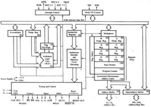
functional units of 8085 microprocessor
8085 की functional unit निम्नलिखित है:-
1:- ALU
ALU का पूरा नाम arithmetic logical unit है. यह numerical और logical ऑपरेशन को परफॉर्म करता है. जैसे:- जोड़ना, घटाना, ‘AND’, ‘OR’ आदि.
यह memory और accumulator से data का प्रयोग arithmetic operation को परफॉर्म करने के लिए करता है. और जो result आता है उसे हमेशा accumulator में store करता है.
ALU के पास accumulator, flag register और temporary registers होते है.
a). Accumulator
accumulator एक 8 bit रजिस्टर होता है जो कि ALU का एक हिस्सा है. इस रजिस्टर का प्रयोग 8 bit डेटा को स्टोर करने के लिए तथा arithmetic और logical ऑपरेशन को पूरा करने के लिए किया जाता है.
इसको कभी कभी register A भी कहते हैं.
b). flag register
8085 के पास 8 bit flag register होता है. इसमें केवल 5 active flags होते है. जैसा कि आप नीचे देख सकते है.
| D7 | D6 | D5 | D4 | D3 | D2 | D1 | D0 |
|---|---|---|---|---|---|---|---|
| S | Z | AC | P | CY |
flags, फ्लिप-फ्लॉप होते है जिनका प्रयोग accumulator तथा दूसरे registers के status को indicate करने के लिए किया जाता है.
ये 5 flags निम्नलिखित है:-
sign flag (S):- sign flag यह indicate करता है कि mathematical और logical ऑपरेशन का result (परिणाम) negative है या positive है.
यदि परिणाम negative होता है तो यह flag set हो जायेगा (अर्थात S=1). और यदि परिणाम positive होता है तो यह flag reset हो जायेगा (अर्थात् S=0).
zero flag (Z):- zero flag यह indicate करता है कि mathematical और logical ऑपरेशन का result (परिणाम) zero (शून्य) है या नही.
यदि वर्तमान operation का परिणाम zero है तो flag set हो जायेगा. (अर्थात Z=1) अन्यथा flag reset हो जायेगा. (अर्थात् Z=0).
इस flag को accumulator और अन्य registers में result के द्वारा modify किया जा सकता है.
Auxiliary carry flag (AC):- एक operation में जब D3 bit के द्वारा carry को generate किया जाता है और उसे D4 को भेज दिया जाता है. तब AC flag SET होगा अन्यथा reset होगा.
इसका प्रयोग केवल BCD operations के लिए ही किया जाता है. और इसमें programmer इसके क्रम को jump instruction के द्वारा नही बदल सकते है.
parity flag (P):- यह फ्लैग यह indicate करता है कि वर्तमान result (परिणाम) even parity है या odd parity.
यदि even parity होता है तो P flag set हो जायेगा अन्यथा reset होगा.
carry flag (CY):- यह फ्लैग यह indicate करता है कि जोड़ने या घटाने के दौरान carry या borrow उत्पन्न होता है या नही.
यदि carry या borrow उत्पन्न होता है तो यह फ्लैग set हो जायेगा अन्यथा reset होगा.
2:- timing and control unit
यह यूनिट सभी operations के लिए timing और control signals उत्पन्न करती है.
यह unit, माइक्रोप्रोसेसर के operations को clock के साथ synchronize करता है तथा माइक्रोप्रोसेसर और peripheral devices के मध्य communication के लिए control signals को उत्पन्न करता है.
नीचे timing और control signals दिए गये है. जो कि internal और external circuits को कंट्रोल करते है:-
- control signals: READY, RD’, WR’, ALE
- status signals: S0, S1, IO/M’
- DMA signals: HOLD, HLDA
- RESET signals: RESET IN, RESET OUT
3:- instruction register and decoder
Instruction register और decoder जो है वह ALU के part होते है. जब instruction मैमोरी से fetch होता है तो यह instruction register (IR) में load हो जाता है.
इसके बाद decoder इस instruction को decode करता है.
IR जो है वह programmable नही होता है. और इसे किसी भी instruction के द्वारा access नही किया जा सकता है.
4:- Register array
8085 के register unit में:-
- 6 general purpose डेटा रजिस्टर होते हैं. (B, C, D, E, H, L)
- दो internal registers होते हैं:- W और Z.
- दो 16-bit address registers होते है:- PC (program counter) और SP (stack pointer).
- एक increment/decrement counter register.
- और एक multiplexer (MUX) होता है.
6 general purpose registers का प्रयोग 8 bit डेटा को स्टोर करने के लिए किया जाता है.
internal registers का प्रयोग instructions के execution के दौरान 8-bit डेटा को hold करने के लिए किया जाता है.
SP का प्रयोग stack memory में स्टोर हुए data के address को point करने के लिए किया जाता है और PC का उपयोग fetch होने वाली अगली instruction को point करने के लिए किया जाता है.
5:- system bus
ये निम्नलिखित तीन प्रकार की होती है:-
a). Data bus:- यह data को बाइनरी के रूप में microprocessor और अन्य external units जैसे मैमोरी के मध्य ले जाती है. इसका size 8 या 16 bits का होता है. यह bi-directional होती है इसमें data flow दोनों तरफ होता है.
b). address bus:- यह operand के address को बाइनरी के रूप में ले जाती है. इसका size 16-bit का होता है. यह unidirectional होती है इसमें data flow केवल एक तरफ होता है.
c). control bus:- control bus जो है वह synchronization signals को ले जाती है और timing signals प्रदान करती है.
6:- Interrupt Control
interrupt एक सिग्नल होता है जो कि माइक्रोप्रोसेसर के routine को suspend कर देता है. और उसे subroutine को परफॉर्म करने के लिए कहता है. और जब subroutine पूरा हो जाता है तो microprocessor वापस main routine पर आ जाता है.
ये interrupts, software और hardware interrupts होते है. कुछ interrupts को ignore किया जा सकता है (maskable). और कुछ interrupts को ignore नही किया जा सकता (non-maskable).
उदाहरण:- INTR, TRAP, RST 7.5, RST 6.5, RST 5.5.
इसे पूरा पढ़ें:- interrupt क्या है और इसके प्रकार क्या है?
7:- Serial I/O control
माइक्रोप्रोसेसर serial data communication को दो instructions के द्वारा control करता है. SID (serial input data) और SOD (serial output data).
निवेदन:- दोस्तों मुझे उम्मीद है कि 8085 microprocessor in hindi की यह article आपके लिए helpful जरुर रहा होगा. इसे आप अपने दोस्तों के साथ share कीजिये और आपके जो भी questions है उन्हें comment के द्वारा बताइए.
This language is very easily & helpful ✌️✌️
A Lot of thanks sir.
a lot of thanks sir.
this notes is good. and very helpful for every student.
very good sir very help full sir
Very very fine all is well description sir
Thank you sir
These are really helpful for me thanx
I got these pages before 2 days of my board exam
Good notes this is important for me.
Thanks sir
you are doing great job upload more topics like timing diagram of microprocessor with details.
एक 16 bit stack pointer होता है.
इसमें 6 (छ), 8 bit registers होते है. जो कि जोड़े में arrange रहते है: BC, PE, HL.
इसको 3.2 MHZ single clock phase में operate करने के लिए +5V power supply की आवश्यकता sir ya samaj nahi aaya